Electronics design
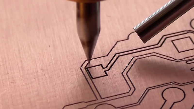
In week 4 we focused on milling and soldering the board, this week I've focused on designing my own PCB board based on the echo hello-world board, which is a micro-controller, while adding an LED and a button as additional components.
What is a circuit?
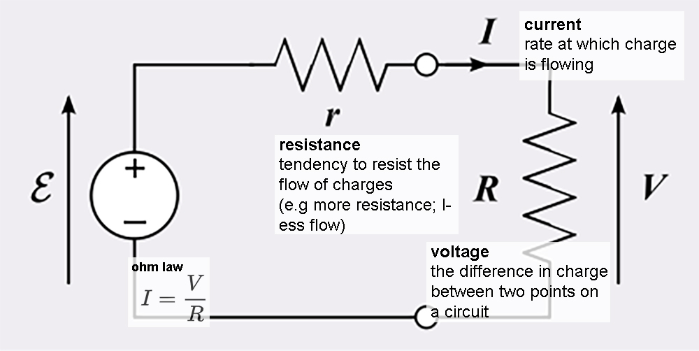
Electricity is the movement of electrons, which creates charges that power up our electronical devices (lightbulbs, phones, etc). A circuit is a closed loop that allows charge to move from one place to another; components in the circuit allows us to have control over the charge.
I used this fantastic tutorial on electronics to get a better grasp on the concepts of voltage, current, resistance, and ohm's law.

What is a microcontroller?
A microcontroller or MCU (NOT Marvel Cinematic Universe) is like a small computer on an integrated circuit. An MCU is usually present in devices and appliances that have an embedded system, which is a system that has a dedicated function within a larger mechanical or electrical system.
Here is a personal explanation of the following components:
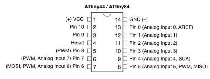
- ATtiny44 (IC1t44): ATtiny44 is our microcontroller, the brains of the operation. It is a programmable component that will dictate what the circuit will do. The ATtiny44 has 14 legs, some of them have specific functions and it is very important to understand which ones are connected to which components. Here's a handy datasheet to understand where these components go:
- VCC (Voltage at the common collector): Where the circuits get their voltage. The voltage comes from an external device.
- GND (Ground): It's the base 0V level
- SCK (Serial Clock): It's used to synchronise the data that is being spoken among the ISP and the microcontroller. The ISP or SPI is an interface bus used to send data between the MCU and peripheral devices such as sensors, SD cards, and shift registers.
- MOSI: Output (SPI)
- MISO: Input (SPI)
- PWM: Pulse Width Modulation: It's used to vary how much time the signal is high in an analog fashion
- AREF: Analogue Reference
- Resistor of 10K Ohm: Used to reduce the flow of the current, we need it to keep steady the flow that goes into the MCU near the VCC and for the reset signal.
- Capacitor 1uF: The capacitor stores voltage that's used to regulate the flow in the circuit in case there are any spikes of current in the voltage.
- FTDI: From here we will connect to the FTDI cable that serves to connect the MCU to a USB port and translate the serial language from the MCU to USB language.
- G (blk): Ground
- CTS: Clear to Send
- VCC: Voltage Common Collector
- Tx: Transmit
- Rx: Receive
- RTS: Request to Send
- Crystal or Resonator (XTAL): This component is an external clock and it emits a signal at certain frequencies (hertz)
- LED+10 OHM resistor: LEDs belong to the diode family. A diode is a component that lets energy flow in only one direction. Alongside the LED we require a resistor, which has the task to limit the current that passes through the circuit in order to not burn the LED. It lowers the voltage to one that the LED bulb can take. In otder to choose the right resistor we need to apply Ohm's Law:
R = V/I (R: Resistor, V: Voltage, I: Current)
The voltage that comes from my computer's USB port is 5V. The current of the LED depends on the model being used, these details can be checked in the Fab Lab Inventory.
Once you know the LED model you can calculate the forward current and forward voltage through here. Turns out I need an 180 Ohm resistor for an LED with 20mA (milliamps) of forward current and 1.75V. - 8. Button: The button serves to turn on and off the LED.
Setting up Eagle
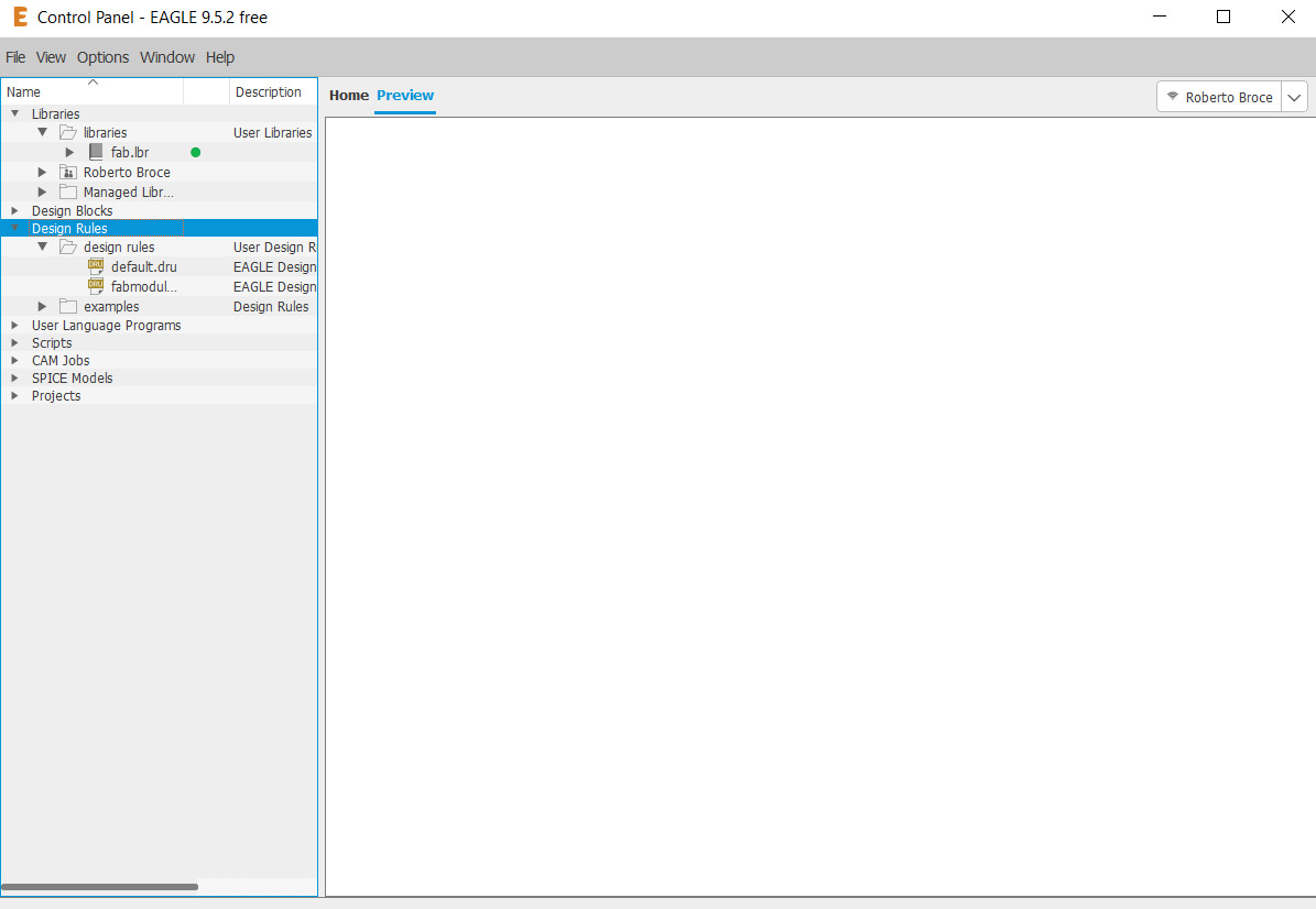
I will be using the software Eagle which is used for PCB design. I will be using materials that every FabLab has in their inventory, therefore I will upload the fab library into our Eagle Library Manager so I can access these materials. Additionally, I will install the fablab design rules which are the settings of the milling machine to properly mill and trace the circuit board. You can download the zip files from this link. The file called "fabmodule.dru" is the one for the design rules, and the file "fab.lbr" for the library of the components. Extract the library and design rules into the Eagle folder in your computer, and afterwards just drag and drop the files under "library" and "design rules".
Then on Eagle, go to Library>Open Library Manager, remove the ones that are inside "IN USE" except for "supply" which you'll need for the VCC and GND parts. It won't delete them just remove from the available components in the library. Then go to AVAILABLE and browse the FAB library and select USE, this will add it to your Eagle library.
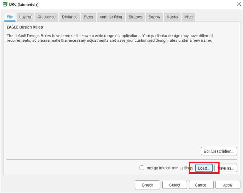
You'll need to load the Design Rules as well. To do that just go to TOOLS>DRC and then load the file of the DESIGN RULES
Creating the schematics
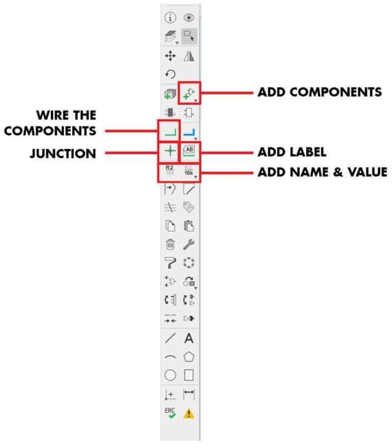
In the schematics window, you can add all of the components you need, based on the hello world reference above. The following are the most important buttons you'll need to remember:
It's important to remember that the schematics are just a floor plan for the circuit board, not a visualisation of the physical components. It doesn't matter where you place the components, what matters is the connection.
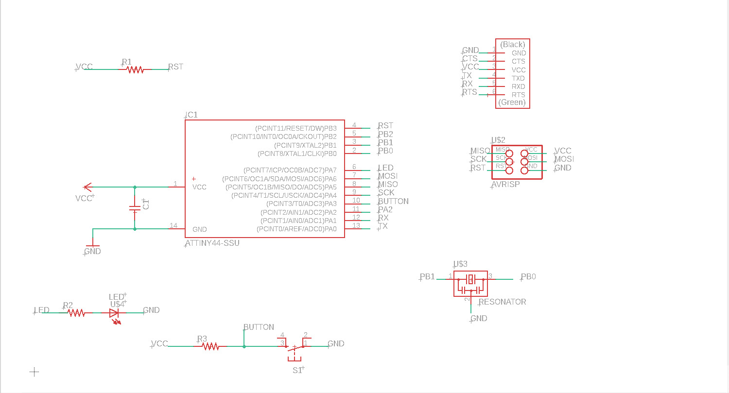
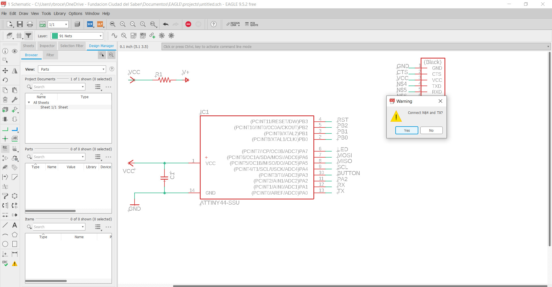
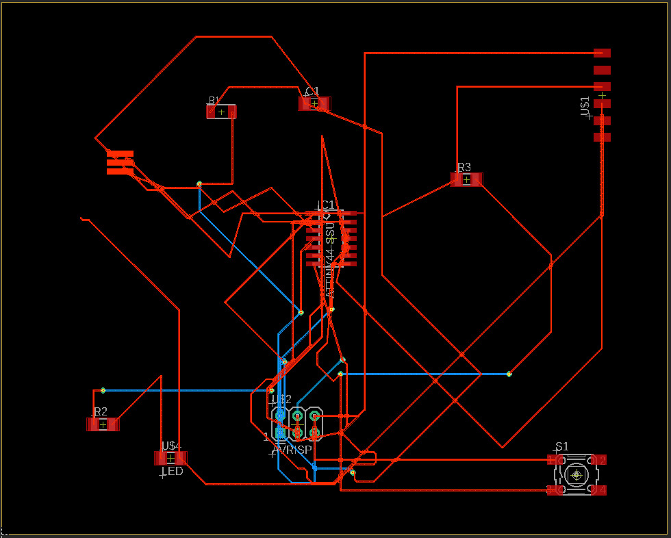
In the schematic, it is useful to add labels to name each extension in the components. Instead of having wires everywhere, you can just label the extension with where it's meant to be connected and the program will connect it for you. It is visually very useful for how easy it is to read the connections.
Generate Board
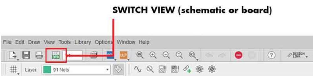
Once all the components are set and linked, we can switch to the board window. The button to switch to the board window is located on the top bar.
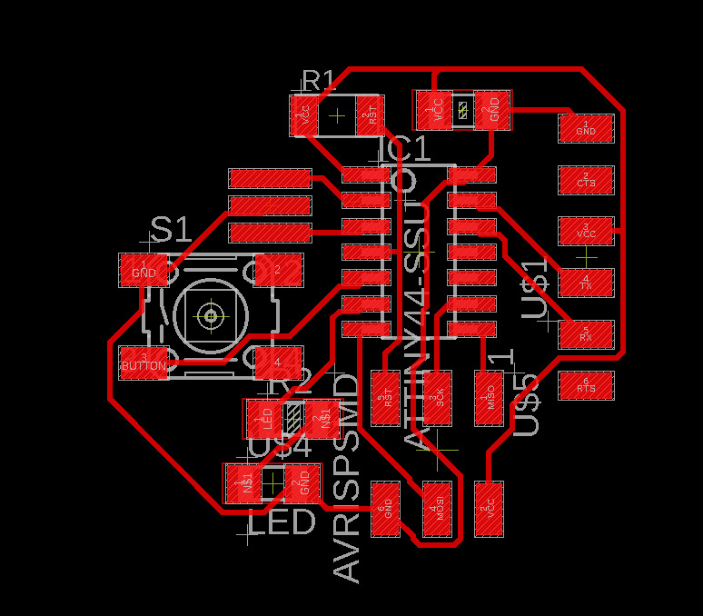
Once you switch to the board window, all the components will be intertwined in the messiest of ways. I tried rearranging them as the program threw it at me but it was too difficult.
This process of rearranging the wires was unnecessarily painful. All the wires were on top of each other and the "autorouter" option barely helped. At the end I decided to delete all of thr wirtes and route it myself, I saved a lot of time. The end result is the image to the left.
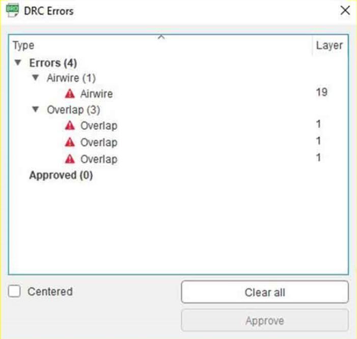
Once the board is readily arranged, turn on the design rules and check that you have no mistakes. The design rules can be activated by going to TOOLS>ERRORS, this will show a window with all the possible errors in the circuit. Airwire means there is no connection, Overlap is when traces are overlapping, Wirestub is when there's a wire on top of another in the component. Make sure you check this and fix all possible errors
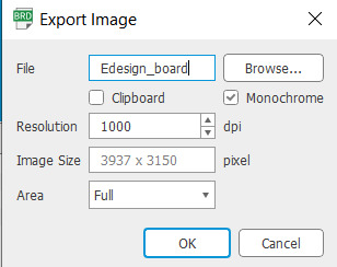
Now turn off all the layers by visiting VIEW>LAYERS SETTINGS and hiding all of the layers except for the top layer. After you've ran the design rules and turned off the layers we're ready to export the image. Go to FILE>EXPORT>IMAGE, the resolution should be 1000dpi and you should choose monochrome.

Preparing the images for milling
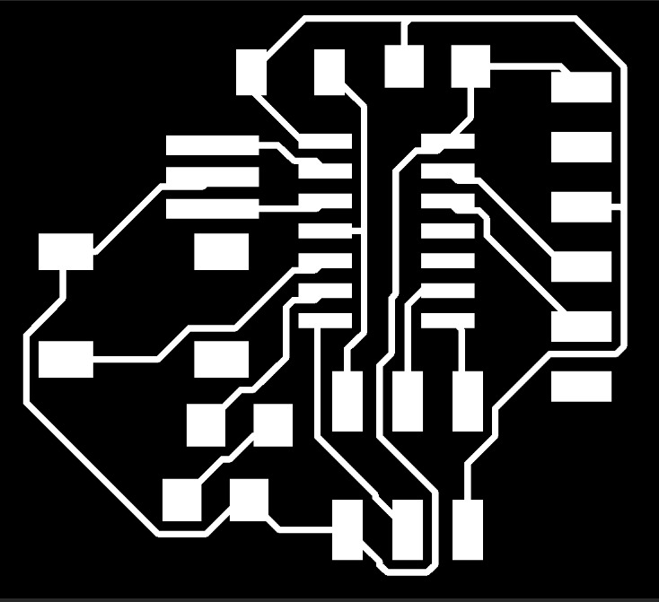
I opened the image on photoshop to add an outline as shown on the image to the left.
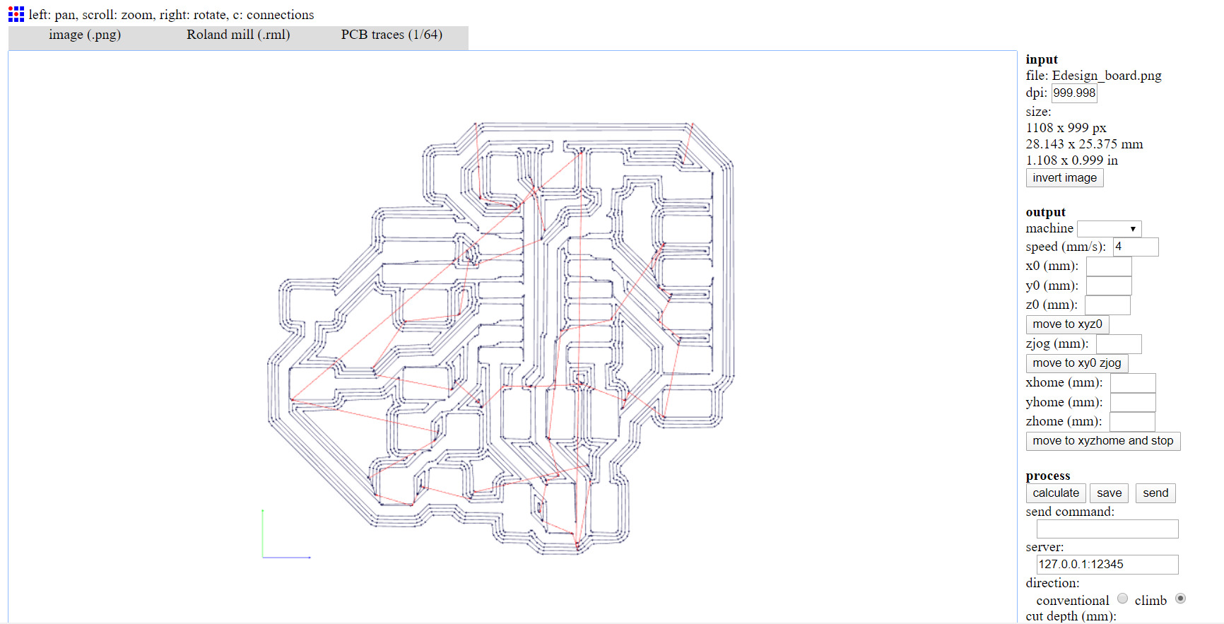
I then opened the image into fabmodules and created some traces: